Amplifier or switch
Bipolar Input/Control Layer/Output
Layers can be N-type (conducts negative) or P-Type (conducts positive).
Layers are formed by treating silicon with traces of impurities.
Boron-produces negative type material-it had a surplus of electrons
Phosphorous produces positive material that has a lack of electrons or surplus of electron holes
The silicon transistor is a semiconductor because it only conducts small amount of current unless a change in voltage occurs at a juncture.
Bi-Polar- input layer emitter
control layer is the base
and the output layer is the collector
When current is applied to the input layer or emitter of an NPN transistor, electrons flow to the P-type base and fill the positive (electron) holes
When holes are filled, it no longer conducts
When a small voltage is applied to the base, it will produce additional holes and allows current to flow from the emitter through the base to the collector.transi
A bipolar transistor consists of a three-layer “sandwich” of doped (extrinsic) semiconductor materials, either P-N-P in Figure below(b) or N-P-N at (d). Each layer forming the transistor has a specific name, and each layer is provided with a wire contact for connection to a circuit.
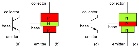
BJT transistor: (a) PNP schematic symbol, (b) physical layout (c) NPN symbol, (d) layout.
The functional difference between a PNP transistor and an NPN transistor is the proper biasing (polarity) of the junctions when operating. For any given state of operation, the current directions and voltage polarities for each kind of transistor are exactly opposite each other.
Bipolar transistors work as current-controlled current regulators. In other words, transistors restrict the amount of current passed according to a smaller, controlling current. The main current that is controlled goes from collector to emitter, or from emitter to collector, depending on the type of transistor it is (PNP or NPN, respectively). The small current that controls the main current goes from base to emitter, or from emitter to base, once again depending on the kind of transistor it is (PNP or NPN, respectively). According to the standards of semiconductor symbology, the arrow always points against the direction of electron flow. (Figure below)

Bipolar transistors are called bipolar because the main flow of electrons through them takes place in two types of semiconductor material: P and N, as the main current goes from emitter to collector (or vice versa). In other words, two types of charge carriers -- electrons and holes -- comprise this main current through the transistor.
As you can see, the controlling current and the controlled current always mesh together through the emitter wire, and their electrons always flow against the direction of the transistor's arrow. This is the first and foremost rule in the use of transistors: all currents must be going in the proper directions for the device to work as a current regulator. The small, controlling current is usually referred to simply as the base current because it is the only current that goes through the base wire of the transistor. Conversely, the large, controlled current is referred to as the collector current because it is the only current that goes through the collector wire. The emitter current is the sum of the base and collector currents, in compliance with Kirchhoff's Current Law.
No current through the base of the transistor, shuts it off like an open switch and prevents current through the collector. A base current, turns the transistor on like a closed switch and allows a proportional amount of current through the collector. Collector current is primarily limited by the base current, regardless of the amount of voltage available to push it. The next section will explore in more detail the use of bipolar transistors as switching elements.
• REVIEW:
• Bipolar transistors are so named because the controlled current must go through two types of semiconductor material: P and N. The current consists of both electron and hole flow, in different parts of the transistor.
• Bipolar transistors consist of either a P-N-P or an N-P-N semiconductor “sandwich” structure.
• The three leads of a bipolar transistor are called the Emitter, Base, and Collector.
• Transistors function as current regulators by allowing a small current to control a larger current. The amount of current allowed between collector and emitter is primarily determined by the amount of current moving between base and emitter.
• In order for a transistor to properly function as a current regulator, the controlling (base) current and the controlled (collector) currents must be going in the proper directions: meshing additively at the emitter and going against the emitter arrow symbol.
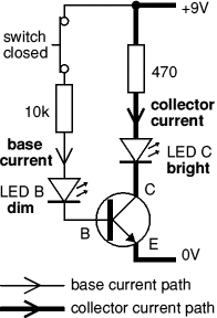 The diagram shows the two current paths through a transistor. You can build this circuit with two standard 5mm red LEDs and any general purpose low power NPN transistor (BC108, BC182 or BC548 for example).
The small base current controls the larger collector current.
When the switch is closed a small current flows into the base (B) of the transistor. It is just enough to make LED B glow dimly. The transistor amplifies this small current to allow a larger current to flow through from its collector (C) to its emitter (E). This collector current is large enough to make LED C light brightly.
When the switch is open no base current flows, so the transistor switches off the collector current. Both LEDs are off.
A transistor amplifies current and can be used as a switch.
This arrangement where the emitter (E) is in the controlling circuit (base current) and in the controlled circuit (collector current) is called common emitter mode. It is the most widely used arrangement for transistors so it is the one to learn first.
The diagram shows the two current paths through a transistor. You can build this circuit with two standard 5mm red LEDs and any general purpose low power NPN transistor (BC108, BC182 or BC548 for example).
The small base current controls the larger collector current.
When the switch is closed a small current flows into the base (B) of the transistor. It is just enough to make LED B glow dimly. The transistor amplifies this small current to allow a larger current to flow through from its collector (C) to its emitter (E). This collector current is large enough to make LED C light brightly.
When the switch is open no base current flows, so the transistor switches off the collector current. Both LEDs are off.
A transistor amplifies current and can be used as a switch.
This arrangement where the emitter (E) is in the controlling circuit (base current) and in the controlled circuit (collector current) is called common emitter mode. It is the most widely used arrangement for transistors so it is the one to learn first.

Functional model of an NPN transistor
The operation of a transistor is difficult to explain and understand in terms of its internal structure.
It is more helpful to use this functional model:
- The base-emitter junction behaves like a diode.
- A base current IB flows only when the voltage VBE
across the base-emitter junction is 0.7V or more.
- The small base current IB controls the large collector current Ic.
- Ic = hFE × IB
(unless the transistor is full on and saturated)
hFE is the current gain (strictly the DC current gain),
a typical value for hFE is 100 (it has no units because it is a ratio)
- The collector-emitter resistance RCE is controlled by the base current IB:
- IB = 0 RCE = infinity transistor off
- IB small RCE reduced transistor partly on
- IB increased RCE = 0 transistor full on ('saturated')
Additional notes:
- A resistor is often needed in series with the base connection to limit the base
current IB and prevent the transistor being damaged.
- Transistors have a maximum collector current Ic rating.
- The current gain hFE can vary widely,
even for transistors of the same type!
- A transistor that is full on (with RCE = 0) is said to be
'saturated'.
- When a transistor is saturated the collector-emitter voltage VCE
is reduced to almost 0V.
- When a transistor is saturated the collector current Ic is determined
by the supply voltage and the external resistance in the collector circuit, not by
the transistor's current gain. As a result the ratio Ic/IB
for a saturated transistor is less than the current gain hFE.
- The emitter current IE = Ic + IB, but Ic
is much larger than IB, so roughly IE = Ic.
There are two types of standard transistors, NPN and PNP, with different circuit symbols. The letters refer to the layers of semiconductor material used to make the transistor. Most transistors used today are NPN because this is the easiest type to make from silicon.
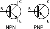
The leads are labelled base (B), collector (C) and emitter (E).
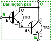
Darlington pair
This is two transistors connected together so that the current amplified by the first is amplified further by the second transistor. The overall current gain is equal to the two individual gains multiplied together:
Darlington pair current gain, hFE = hFE1 × hFE2
(hFE1 and hFE2 are the gains of the individual transistors)
This gives the Darlington pair a very high current gain, such as 10000, so that only a tiny base current is required to make the pair switch on.
A Darlington pair behaves like a single transistor with a very high current gain. It has three leads (B, C and E) which are equivalent to the leads of a standard individual transistor. To turn on there must be 0.7V across both the base-emitter junctions which are connected in series inside the Darlington pair, therefore it requires 1.4V to turn on.
Darlington pairs are available as complete packages but you can make up your own from two transistors; TR1 can be a low power type, but normally TR2 will need to be high power. The maximum collector current Ic(max) for the pair is the same as Ic(max) for TR2.
A Darlington pair is sufficiently sensitive to respond to the small current passed by your skin and it can be used to make a touch-switch as shown in the diagram. For this circuit which just lights an LED the two transistors can be any general purpose low power transistors. The 100k resistor protects the transistors if the contacts are linked with a piece of wire.
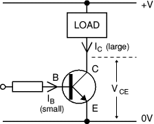
Using a transistor as a switch
When a transistor is used as a switch it must be either OFF or fully ON. In the fully ON state the voltage VCE across the transistor is almost zero and the transistor is said to be saturated because it cannot pass any more collector current Ic. The output device switched by the transistor is usually called the 'load'.
The power developed in a switching transistor is very small:
In the OFF state: power = Ic × VCE, but Ic = 0, so the power is zero.
In the full ON state: power = Ic × VCE, but VCE = 0 (almost), so the power is very small.
This means that the transistor should not become hot in use and you do not need to consider its maximum power rating. The important ratings in switching circuits are the maximum collector current Ic(max) and the minimum current gain hFE(min). The transistor's voltage ratings may be ignored unless you are using a supply voltage of more than about 15V. There is a table showing technical data for some popular transistors on the transistors page.
For information about the operation of a transistor please see the functional model above.
Protection diode
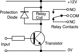
If the load is a motor, relay or solenoid (or any other device with a coil) a diode must be connected across the load to protect the transistor from the brief high voltage produced when the load is switched off. The diagram shows how a protection diode is connected 'backwards' across the load, in this case a relay coil.
A transistor can also be used to enable an IC connected to a low voltage supply (such as 5V)
to switch the current for an output device with a separate higher voltage supply (such as 12V).
The two power supplies must be linked, normally this is done by linking their 0V connections.
In this case you should use an NPN transistor.
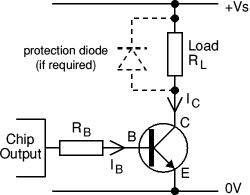
A resistor RB is required to limit the current flowing into the base of the
transistor and prevent it being damaged. However, RB must be sufficiently low to
ensure that the transistor is thoroughly saturated to prevent it overheating, this is
particularly important if the transistor is switching a large current (> 100mA).
A safe rule is to make the base current IB about five times larger than
the value which should just saturate the transistor.
Choosing a suitable NPN transistor
The circuit diagram shows how to connect an
NPN transistor, this will switch on
the load when the IC output is
high. If you need the opposite
action, with the load switched on when the IC output is
low (0V) please
see the circuit for a
PNP transistor below.
The procedure below explains how to choose a suitable switching transistor.
- The transistor's maximum collector current Ic(max)
must be greater than the load current Ic.
| load current Ic = |
supply voltage Vs |
| load resistance RL |
- The transistor's minimum current gain hFE(min)
must be at least five times the load current Ic divided
by the maximum output current from the IC.
| hFE(min) > 5 × |
load current Ic |
| max. IC current |
- Choose a transistor which meets these requirements and make a note of
its properties: Ic(max)
and hFE(min).
There is a table showing technical data for some popular transistors
on the transistors page.
- Calculate an approximate value for the base resistor:
| RB = |
Vc × hFE |
where Vc = IC supply voltage
(in a simple circuit with one supply this is Vs) |
| 5 × Ic |
For a simple circuit where the IC and the load share the same power supply
(Vc = Vs) you may prefer to use:
RB = 0.2 × RL × hFE
Then choose the nearest standard value for the base resistor.
- Finally, remember that if the load is a motor or relay coil a
protection diode is required.
Example
The output from a 4000 series CMOS IC is required to operate a relay with a
100 coil.
coil.
The supply voltage is 6V for both the IC and load. The IC can supply a maximum current of 5mA.
- Load current = Vs/RL = 6/100 = 0.06A = 60mA,
so transistor must have Ic(max) > 60mA.
- The maximum current from the IC is 5mA,
so transistor must have hFE(min) > 60
(5 × 60mA/5mA).
- Choose general purpose low power transistor BC182 with
Ic(max) = 100mA
and hFE(min) = 100.
- RB = 0.2 × RL × hFE
= 0.2 × 100 × 100 =
2000.
so choose RB = 1k8 or 2k2.
- The relay coil requires a protection diode.
Choosing a suitable PNP transistor
The circuit diagram shows how to connect a
PNP transistor, this will switch on
the load when the IC output is
low (0V). If you need the opposite
action, with the load switched on when the IC output is
high please
see the circuit for an
NPN transistor above.
The procedure for choosing a suitable PNP transistor is exactly the same
as that for an NPN transistor described above.
Using a transistor switch with sensors
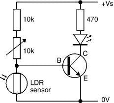 |
| LED lights when the LDR is dark |
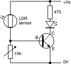 |
LED lights when the LDR is bright
|
The top circuit diagram shows an
LDR (light sensor)
connected so that the LED lights when the LDR is in darkness.
The variable resistor adjusts the brightness at which the transistor switches on and off.
Any general purpose low power transistor can be used in this circuit.
The 10k fixed resistor
protects the transistor from excessive base current (which will destroy it) when the variable
resistor is reduced to zero. To make this circuit switch at a suitable brightness you may
need to experiment with different values for the fixed resistor, but it must not be less than
1k.
If the transistor is switching a load with a coil, such as a motor or relay, remember
to add a protection diode across the load.
The switching action can be inverted, so the LED lights when the
LDR is brightly lit, by swapping the LDR and variable resistor. In this case the fixed
resistor can be omitted because the LDR resistance cannot be reduced to zero.
Note that the switching action of this circuit is not particularly good because there will
be an intermediate brightness when the transistor will be partly on (not saturated).
In this state the transistor is in danger of overheating unless it is switching a
small current. There is no problem with the small LED current, but the larger current
for a lamp, motor or relay is likely to cause overheating.
Other sensors, such as a thermistor,
can be used with this circuit, but they may require a different variable resistor.
You can calculate an approximate value for the variable resistor (Rv) by using a
multimeter to find the minimum and maximum values
of the sensor's resistance (Rmin and Rmax):
Variable resistor, Rv = square root of (Rmin × Rmax)
For example an LDR: Rmin =
100, Rmax =
1M, so Rv =
square root of (100 × 1M)
= 10k.
You can make a much better switching circuit with sensors connected to a suitable
IC (chip). The switching action will be much sharper with no partly on state.
A transistor inverter (NOT gate)
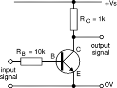
Inverters (NOT gates) are available on logic ICs but if you only require one
inverter it is usually better to use this circuit. The output signal (voltage)
is the inverse of the input signal:
- When the input is high (+Vs) the output is low (0V).
- When the input is low (0V) the output is high (+Vs).
Any general purpose low power NPN transistor can be used. For general use
R
B = 10k
and R
C = 1k
,
then the inverter output can be connected to a device with an input impedance (resistance)
of at least 10k
such as a logic IC or a 555 timer (trigger and reset inputs).
If you are connecting the inverter to a CMOS logic IC input (very high impedance)
you can increase RB to
100k
and RC to 10k,
this will reduce the current used by the inverter.
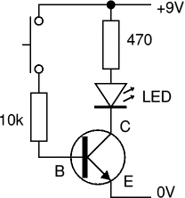
Testing in a simple switching circuit
Connect the transistor into the circuit shown on the right which uses the transistor as a switch.
The supply voltage is not critical, anything between 5 and 12V is suitable.
This circuit can be quickly built on
breadboard for example.
Take care to include the 10k

resistor in the base connection or you will destroy the transistor as you test it!
If the transistor is OK the LED should light when the switch is pressed
and not light when the switch is released.
To test a PNP transistor use the same circuit but reverse the LED and the supply voltage.
Some multimeters have a 'transistor test' function which
provides a known base current and measures the collector current so as to display the
transistor's DC current gain hFE.
Transistor codes
There are three main series of transistor codes used in the UK:
- Codes beginning with B (or A), for example BC108, BC478
The first letter B is for silicon, A is for germanium (rarely used now).
The second letter indicates the type; for example C means low power audio frequency;
D means high power audio frequency; F means low power high frequency.
The rest of the code identifies the particular transistor.
There is no obvious logic to the numbering system.
Sometimes a letter is added to the end (eg BC108C) to identify a special version
of the main type, for example a higher current gain or a different case style.
If a project specifies a higher gain version (BC108C) it must be used,
but if the general code is given (BC108) any transistor with that code is suitable.
- Codes beginning with TIP, for example TIP31A
TIP refers to the manufacturer: Texas Instruments Power transistor.
The letter at the end identifies versions with different voltage ratings.
- Codes beginning with 2N, for example 2N3053
The initial '2N' identifies the part as a transistor and the rest of the code
identifies the particular transistor.
There is no obvious logic to the numbering system.
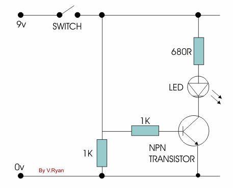
The circuit shown in diagram B is based on an NPN transistor. When the switch is pressed a current passes through the resistor into the base of the transistor. The transistor then allows current to flow from the +9 volts to the 0vs, and the lamp comes on.
The transistor has to receive a voltage at its ‘base’ and until this happens the lamp does not light.
The resistor is present to protect the transistor as they can be damaged easily by too high a voltage / current. Transistors are an essential component in many circuits and are sometimes used to amplify a signal.
Source:www.kpsec.freeuk.com/trancirc.htm
http://www.technologystudent.com/elec1/transis1.htm
http://www.allaboutcircuits.com/vol_3/chpt_4/1.html